 | –≠–ª–µ–∫—Ç—Ä–æ–Ω–Ω—ã–π –∫–æ–º–ø–æ–Ω–µ–Ω—Ç: LM317L | –°–∫–∞—á–∞—Ç—å:  PDF PDF  ZIP ZIP |

1/10
February 2003
s
OUTPUT VOLTAGE RANGE: 1.2 TO 37V
s
OUTPUT CURRENT IN EXCESS OF 100 mA
s
LINE REGULATION TYP. 0.01%
s
LOAD REGULATION TYP. 0.1%
s
THERMAL OVERLOAD PROTECTION
s
SHORT CIRCUIT PROTECTION
s
OUTPUT TRANSISTOR SAFE AREA
COMPENSATION
s
FLOATING OPERATION FOR HIGH
VOLTAGE APPLICATIONS
DESCRIPTION
The LM217L/LM317L are monolithic integrated
circuit in SO-8 and TO-92 packages intended for
use as positive adjustable voltage regulators.
They are designed to supply until 100 mA of load
current with an output voltage adjustable over a
1.2 to 37V range.
The nominal output voltage is selected by means
of only a resistive divider, making the device
exceptionally easy to use and eliminating the
stocking of many fixed regulators
LM217L
LM317L
LOW CURRENT
1.2 TO 37V ADJUSTABLE VOLTAGE REGULATOR
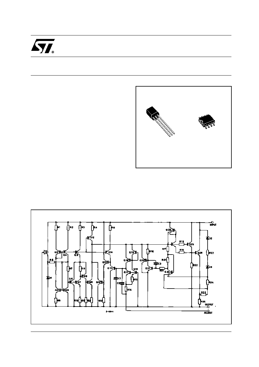
SCHEMATIC DIAGRAM
TO-92
SO-8

LM217L/LM317L
2/10
ABSOLUTE MAXIMUM RATINGS
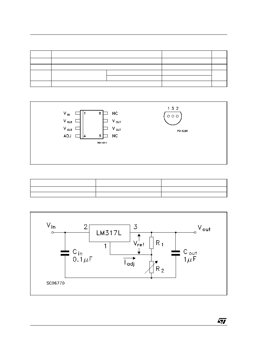
CONNECTION DIAGRAM (top view)
ORDERING CODES
TEST CIRCUIT
Symbol
Parameter≤
Value
Unit
V
I -
V
O
Input-Output Differential Voltage
40
V
P
d
Power Dissipation
Internally Limited
T
opr
Operating Junction Temperature
Range
for LM217L
-40 to 125
∞C
for LM317L
0 to 125
T
stg
Storage Temperature Range
-55 to 150
∞C
TYPE
SO-8
TO-92
LM217L
LM217LD
LM217LZ
LM317L
LM317LD
LM317LZ
SO-8
TO-92
PIN 1 = ADJUST
PIN 2 = IN
PIN 3 = OUT
BOTTOM VIEW

LM217L/LM317L
3/10
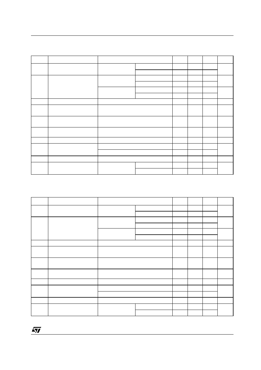
ELECTRICAL CHARACTERISTICS OF LM217L (refer to the test circuits, T
J
= - 40 to 125∞C,
V
I
- V
O
= 5 V, I
O
= 40 mA, unless otherwise specified).
(*) CADJ is connected between Adjust pin and Ground.
ELECTRICAL CHARACTERISTICS OF LM317L (refer to the test circuits, T
J
= 0 to 125∞C,
V
I
- V
O
= 5 V, I
O
= 40 mA, unless otherwise specified).
(*) CADJ is connected between Adjust pin and Ground.
Symbol
Parameter
Test Conditions
Min.
Typ.
Max.
Unit
V
O
Line Regulation
V
I
- V
O
= 3 to 40 V
I
L
< 20 mA
T
J
= 25∞C
0.01
0.02
%/V
0.02
0.05
V
O
Load Regulation
V
O
5 V
I
O
= 5 to 100 mA
T
J
= 25∞C
5
15
mV
20
50
V
O
5 V
I
O
= 5 to 100 mA
T
J
= 25∞C
0.1
0.3
%
0.3
1
I
ADJ
Adjustment Pin Current
50
100
µA
I
ADJ
Adjustment Pin Current
V
I
- V
O
= 3 to 40 V I
O
= 5 to 100 mA
P
d
< 625 mW
0.2
5
µA
V
REF
Reference Voltage
V
I
- V
O
= 3 to 40 V I
O
= 10 to 500 mA
P
d
< 625 mW
1.2
1.25
1.3
V
V
O
/V
O
Output Voltage
Temperature Stability
0.7
%
I
O(min)
Minimum Load Current
V
I
- V
O
= 40 V
3.5
5
mA
I
O(max)
Maximum Output Current
V
I
- V
O
= 3 to 13 V
100
200
mA
V
I
- V
O
= 40 V
50
eN
Output Noise Voltage
B = 10 Hz to 10 KHzT
J
= 25∞C
0.003
%
SVR
Supply Voltage Rejection (*) T
J
= 25∞C
f = 120 Hz
C
ADJ
= 0
65
dB
C
ADJ
= 10 µF
66
80
Symbol
Parameter
Test Conditions
Min.
Typ.
Max.
Unit
V
O
Line Regulation
V
I
- V
O
= 3 to 40 V
I
L
< 20 mA
T
J
= 25∞C
0.01
0.04
%/V
0.02
0.07
V
O
Load Regulation
V
O
5 V
I
O
= 5 to 100 mA
T
J
= 25∞C
5
25
mV
20
70
V
O
5 V
I
O
= 5 to 100 mA
T
J
= 25∞C
0.1
0.5
%
0.3
1.5
I
ADJ
Adjustment Pin Current
50
100
µA
I
ADJ
Adjustment Pin Current
V
I
- V
O
= 3 to 40 V I
O
= 5 to 100 mA
P
d
< 625 mW
0.2
5
µA
V
REF
Reference Voltage
V
I
- V
O
= 3 to 40 V I
O
= 5 to 100 mA
P
d
< 625 mW
1.2
1.25
1.3
V
V
O
/V
O
Output Voltage
Temperature Stability
0.7
%
I
O(min)
Minimum Load Current
V
I
- V
O
= 40 V
3.5
5
mA
I
O(max)
Maximum Output Current
V
I
- V
O
= 3 to 13 V
100
200
mA
V
I
- V
O
= 40 V
50
eN
Output Noise Voltage
B = 10 Hz to 10 KHzT
J
= 25∞C
0.003
%
SVR
Supply Voltage Rejection (*) T
J
= 25∞C
f = 120 Hz
C
ADJ
= 0
65
dB
C
ADJ
= 10 µF
66
80

LM217L/LM317L
4/10
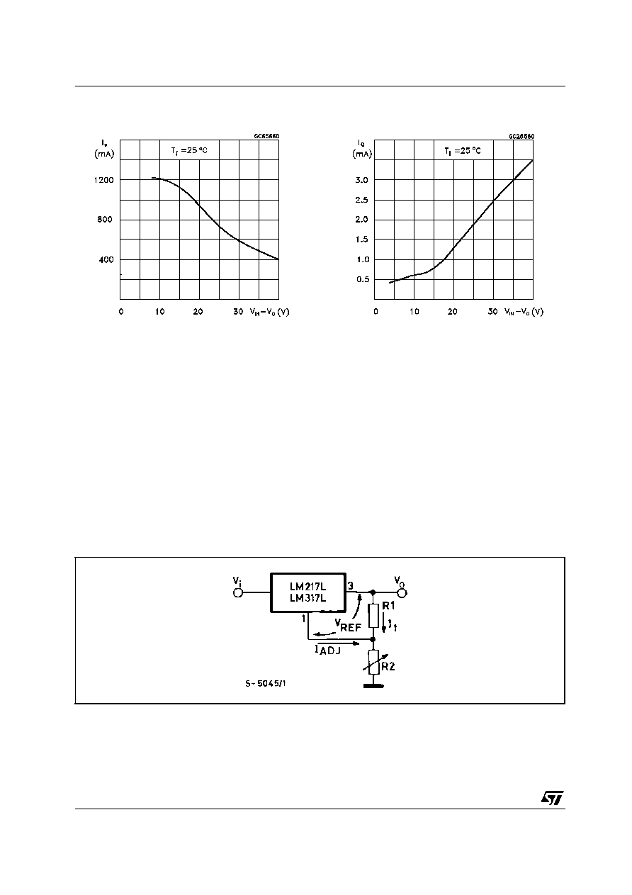
Figure 1 : Current Limit
Figure 2 : Minimum Operating Current
APPLICATION INFORMATION
The LM317L provides an internal reference voltage of 1.25V between the output and adjustments
terminals. This is used to set a constant current flow across an external resistor divider (see fig. 4), giving
an output voltage V
O
of:
V
O
= V
REF
(1 + R
2
/R
1
) + I
ADJ
R
2
The device was designed to minimize the term I
ADJ
(100µA max) and to maintain it very constant with line
and load changes. Usually, the error term I
ADJ
◊ R
2
can be neglected. To obtain the previous requirement,
all the regulator quiescent current is returned to the output terminal, imposing a minimum load current
condition. If the load is insufficient, the output voltage will rise.
Since the LM317L is a floating regulator and "sees" only the input-to-output differential voltage, supplies
of very high voltage with respect to ground can be regulated as long as the maximum input-to-output
differential is not exceeded. Furthermore, programmable regulator are easily obtainable and, by
connecting a fixed resistor between the adjustment and output, the device can be used as a precision
current regulator. In order to optimize the load regulation, the current set resistor R
1
(see fig. 4) should be
tied as close as possible to the regulator, while the ground terminal of R
2
should be near the ground of the
load to provide remote ground sensing.
Figure 3 : Basic Adjustable Regulator

LM217L/LM317L
5/10
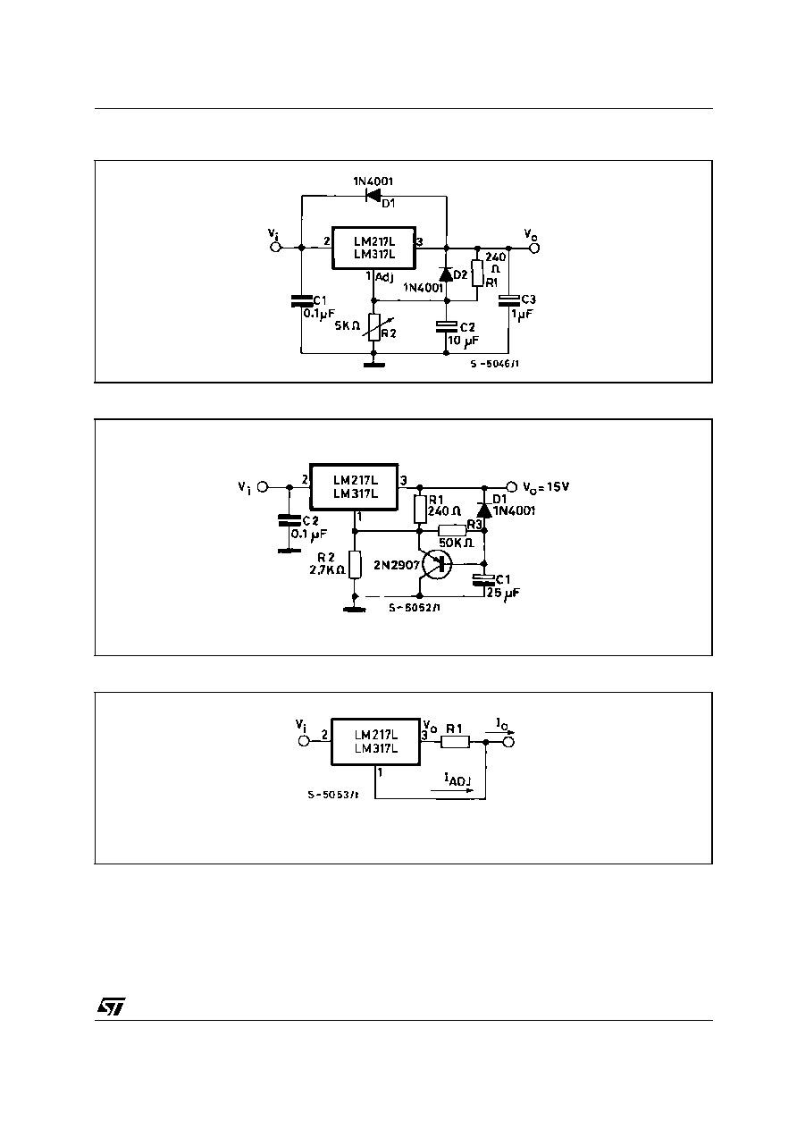
Figure 4 : Voltage Regulator with Protection Diodes
Figure 5 : Slow Turn-on 15V Regulator
Figure 6 : Current Regulator
1.25V
R
1
V
ref
I
O
=
+
I
ADJ
R
1
